Mask Design Method to Control Film Thickness Uniformity on Spherical Substrates
With Progressing of 193 nm micro-lithography systems to high numerical aperture (NA), some elements of the optical imaging systems present large clear aperture (CA) exceeding 300 mm and high ratio of CA to radius of curvature (CA/RoC). Film thickness uniformity for the lenses is greatly decreased, and the performances of the optical lithography systems are influenced eventually.
Improving film thickness uniformity over spherical substrates is one of the crucial factors for coating of optical lithography systems.Film thickness uniformity is realized by shadowing masks in planetary rotation coating plant. Traditionally, the shadowing masks are realized by error and trail method experimentally, which increase the time and cost for optical coatings greatly.
The researchers from Institute of Optics and Electronics developed new methods to design shadowing masks straightforwardly based on computer assisted procedure. They simulated the coating process and designed the shadowing masks theoretically to improve film thickness uniformity. Researchers found relationship between the shape of the shadowing masks and the film thickness distribution of the spherical substrates. So the shapes of shadowing masks are determined basically. The size of shadowing masks is related to single parameter, which is obtained from local optimization procedure. Using this method, film thickness uniformity of a flat substrate with diameter 400mm is improved to 99.6% with a single experiment. The method works well for spherical substrates and improving the film thickness to above 97% with a single experiment. The research is of great importance for development of computer assisted coating technique and film thickness uniformity improvement on other optical systems.
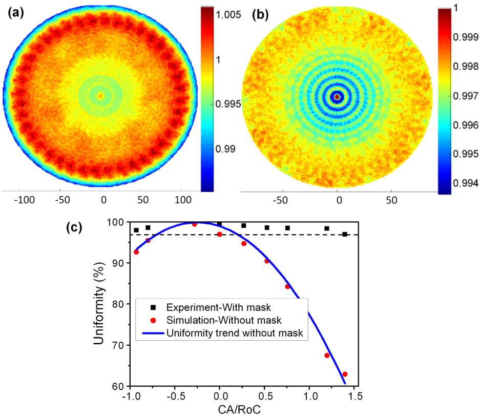
Film thickness uniformity after correction on (a) a steep convex substrate, and (b) a steep concave substrate. (c) film thickness uniformity of spherical substrate with different CA/RoC before and after film thickness correction. (Plotted by LIU Cunding)
Contact:
Sun Qiuyan
E-mail: ioesqy@ioe.ac.cn
Thin-film Optics Laboratory, Institute of Optics and Electronics (http://english.ioe.cas.cn/)