Nanopatterned WS2 Monolayers Enable Subnanometer-thick Optical Holograms
A nanopatterned 2D transition metal dichalcogenide (TMD) monolayer, illuminated by near-infrared laser light, creates an ultrathin transmission hologram via nonlinear second harmonic generation.
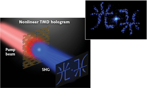
Scientists at Missouri University of Science and Technology (Rolla, MO) have created what they say are the thinnest optical holograms to date using only one tungsten disulfide (WS2) monolayer, itself only about 0.7 nm thick. Using focused-ion-beam milling, pre-designed hologram patterns with binary amplitude modulation of zero and one are directly etched into the WS2 monolayer—a transition metal dichalcogenide (TMD) material—that has been deposited on a sapphire substrate. By exciting the nanopatterned monolayer with a near-infrared ultrafast laser, the reconstructed holographic images in visible wavelengths are obtained in the transmitted signals through the same nonlinear optical process of second-harmonic generation that is also used to produce vortex and Airy beams and other complex images.
Not only do these TMD transmission holograms have high nonlinear conversion efficiencies on the order of 10-6 to 10-5 (much higher than that for the currently existing plasmonic metasurface holograms on the order of 10-11 to 10-9), but they also have an atomic thickness of less than 1 nm—far thinner than the tens of nanometers for plasmonic metasurfaces and hundreds of nanometers for dielectric metasurfaces. This new concept for fabricating atomically thin optical holograms with 2D material monolayers will enable new applications in 3D displays for smart watches, security markings on credit cards and banknotes, and even for high-density data storage. Reference: A. Dasgupta, J. Gao, and X. Yang, Nano Lett., 19, 9, 6511–6516 (Aug. 16, 2019).
(From:https://www.laserfocusworld.com/optics/article/14040321/nanopatterned-ws2-monolayers-enable-subnanometerthick-optical-holograms)