Optical Antennas: Bundt-pan-shaped Optenna Demonstrates 80 dB Infrared Concentration
An optical antenna fabricated in the shape of a Bundt pan can concentrate energy over targeted infrared wavelength bands by up to 8 orders of magnitude.
Attempts to miniaturize radiation-collecting devices such as photodetectors and solar cells often result in poor collection efficiency; however, a variety of plasmonic nanoscale optical antennas made with gold nanoparticles and 2D graphene layers and with horn shapes and circular and spiral arrays, for example, have been fabricated that can concentrate infrared (IR) energy over various wavelength bands by up to seven orders of magnitude.
Improving on existing designs by demonstrating 80 dB (eight orders of magnitude) polarization-insensitive IR concentration in each of the near-IR (NIR), short-wavelength IR (SWIR), and mid-IR (MWIR) bands is a tube- or Bundt-pan-shaped optical antenna developed by professor Ehab Awad at King Saud University (Riyadh, Saudi Arabia). The conical shape of the device creates a large aperture that allows it to gather radiation from an 80° wide field of view.
The recipe
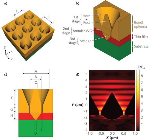
On a bulk silicon substrate, a 700-nm-thick silicon nitride (Si3N4) IR absorbing layer is topped with conical, horn, and waveguide structures that constitute one Bundt-shaped cell (see figure). A series of these cells is built into an array with physical parameters optimized through 3D finite-difference time-domain (FDTD) simulations to maximize radiation capture over a particular IR wavelength range through impedance matching between free space and the array.
Each Bundt-shaped structure has a gold conical horn region that focuses IR energy by exciting surface plasmon polaritons (SPPs) on the conical surfaces and funnels the TE11 mode energy down to a vertical waveguide structure with 50 nm width in a ring shape at the base of the Bundt structure. The array has a central cone-to-cone separation L and each Bundt structure has a depth and diameter optimized to concentrate a NIR, SWIR, or MWIR wavelength band (for example, the MWIR-optimized array has center-to-center L = 3.25 μm, Bundt-pan outer diameter A = 3.2 μm, conical-region Bundt-pan depth E = 5 μm, and waveguide depth G = 1 μm). The 50 nm waveguide width and 700 nm absorbing layer thickness are fixed for all designs.
Simulations show that the eight-orders-of-magnitude concentrated IR energy is funneled via the waveguides onto an annular ring structure that terminates at the absorbing IR material layer and is rapidly attenuated in the absorber.
“The Bundt optenna is promising for nanoscale IR detection devices such as solar cells, telecommunications photodetectors, shortwave cameras, and midwave microbolometers,” says Awad. “During the optenna design and optimization process of trying to reach peak performance, it was surprising to find out that the best optenna shape looks like a Bundt cake pan.”
(From:https://www.laserfocusworld.com/detectors-imaging/article/14040152/bundtpanshaped-optenna-demonstrates-80-db-infrared-concentration)