Beam Shaping Enables New Laser Surface Treatment Applications
Technology provides missing link between technical challenges and innovations
DIRK HAUSCHILD
Thanks to the race to lower costs that has taken place in the laser industry over the last decade, power and wavelength are available from the ultraviolet to infrared for a just a few U.S. dollars per watt. This trend is driven by critical laser applications in the steel and electronics industries. By combining the extremely attractive cost and performance structure of laser sources with beam shaping technologies that allow the use of nearly 100% of the photons in high added-value materials refining and synthesis, a new wave of innovations will provide solutions with potentially game-changing levels of high performance.
The most prominent example involving the use of beam shaping technologies in industry is the transformation of a circular beam into a line beam profile. With this small change, surfaces can be heated up to 20X more efficiently than with a typical circular beam and 2D scanner. The simple physics behind this effect is the linear thermal diffusion within the line beam instead of the radial thermal diffusion of a circular beam profile (FIGURE 1). This effect becomes even more significant where continuous-wave (CW) laser sources are used for surface and thin-film heat treatment.
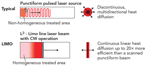
FIGURE 1. A comparison of material heating using a circular and a line-shaped beam is shown.
This technology has already been in use for several years in the selective hardening of metal surfaces and metal coatings with a typical dwell time of a few seconds and a heat-affected zone (HAZ) of a few millimeters. If the line beam is moved over the surface at a significantly higher speed, the dwell time can be shortened into the millisecond range, with HAZ from the micron scale down to a few hundred nanometers.
With this type of selective heating process, the surfaces and coatings can be heat-treated at much higher temperatures than with the typical isothermal processes used in furnaces. The resulting new degree of surface engineering freedom enables the use of materials and material composites otherwise not available for the typical heating processes limited by the damage threshold of the substrate materials.
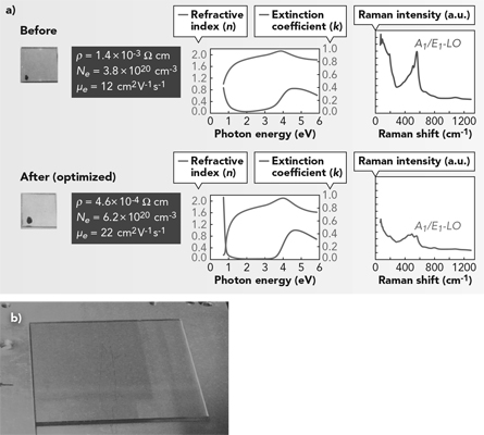
FIGURE 2. (a) Laser annealing of transparent conducting oxide (TCO) enables higher transmission and lower resistivity (Courtesy: EMRS Spring Meeting, Symposium Y, Strasbourg, France, May 17, 2012); (b) shows line beam laser annealing of TCO with an Activation Line 12 system.
Beam shaping applications
The first group of applications consists of solid phase material-refining processes that utilize the annealing of semiconductors and conductors to improve electron mobility and free-carrier concentration for highly efficient electronic devices (FIGURE 2), as well as low-ohmic conductor tracks for printed electronics and high-efficiency power transmission via cables or antennas on polymer, paper, or glass (FIGURE 3). The CW line beam process was able to use not only expensive nanosilver, but also copper-based inks with a layer thickness measuring up to several microns.
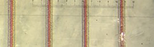
FIGURE 3. Printed and laser-sintered copper wires on polymer using the Fraunhofer Institute for Ceramic Technologies and Systems’ metal inks and pastes are shown.
The second group is composed of liquid phase material-refining processes using crystallization, defined dewetting, and decomposition processes to equip high-performance coatings with a host of improved features and new synthesized material properties. The laser liquid phase crystallization (LLPC) of silicon with layer thicknesses of up to 20 μm is already capable of achieving the same electronic performance as polycrystalline photovoltaic wafers.
The latest results from the collaboration with Helmholtz Center Berlin show a nearly monocrystalline quality that was achieved with an Activation Line CW diode laser system (FIGURE 4). Thanks to the customizable dwell time and power, it was possible to accurately set the process window with the best grain quality and size, which is a unique feature of the LLPC heating process based on the CW line beam laser.
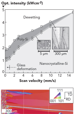
FIGURE 4. Laser liquid phase crystallization (LLPC) of silicon using a CW line beam laser is shown. (Adapted from S. Kühnapfel et al.)
Dewetting is another liquid phase process. Depending on the specific line beam parameter, it is possible to dewet using a stochastic (FIGURE 5) or regular pattern (FIGURE 6). Using simulations, it is possible to design the line beam process in a more specific way and thereby obtain a regular dewetted pattern of semiconductor or metal droplets, for example. The size and pitch of the droplets depend solely on the layer material, the line beam parameter, and the dwell time defined by the line width and movement speed of the line and the target.
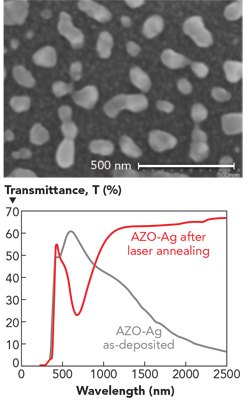
FIGURE 5. Stochastic dewetting of a nanosilver layer with plasmonic optical performance is shown. (Courtesy: RainbowEnergy Project, BMBF, TüBITAK)
The last example of a liquid phase process using defined heating with a line beam focuses on the spinoidal decomposition of silicon-rich oxide (SiO) that generates nanoscale structures with quantum confinement effects and sponge-like mechanical structures. Because the typical furnace-based process takes several hours and is therefore too slow and too expensive, an international team based in Turkey and Germany developed a new way of creating this material (the RainbowEnergy project).
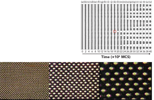
FIGURE 6. Simulation and production of a regular dewetted pattern using line beam laser processing is shown.
First, the mechanisms of the spinoidal decomposition were simulated to get an idea of the speed and the accompanying temperature necessary for speeding up the process from a matter of hours to a span of milliseconds (FIGURE 7). By raising the process temperature to over 1200°C, the speed of this process was increased to make it compatible with high-speed inline processes using dwell times <50 ms and a line-shaped CW laser source (FIGURE 8).
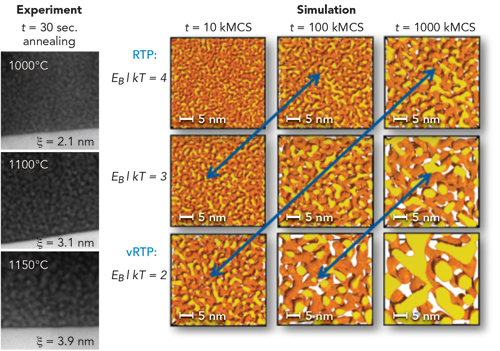
FIGURE 7. Simulation of the spinoidal decomposition of silicon-rich oxide (SiO) into sponge-like nanocrystalline silicon is shown. (Courtesy: RainbowEnergy Project, BMBF, TüBITAK)
This example of designing a material and a process window on the computer and using a laser with a line-shaped beam profile to produce the new high-performing structure provides an impressive first glimpse into the potential of this technology and the new flexibility for the use of laser sources in the development and production of new materials and new material properties. A technology capable of creating specific material properties could be the missing link needed to solve many current challenges in fields including the generation, transmission, and storage of electrical energy.
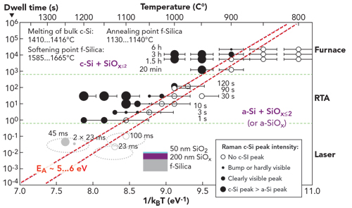
FIGURE 8. Spinoidal decomposition of SiO into c-Si from hours to milliseconds is shown. (Courtesy: RainbowEnergy Project, BMBF, TüBITAK)
Future benefits
Adding specific functionality to a substrate material that has always been unable to withstand the required isothermal process temperature, and doing so at a much higher temperature with millisecond line beam laser heating, is an intriguing prospect for many industries and applications. And if productivity needs to be scaled, a longer line beam can enable processing speeds of several square meters per minute, or even per second, using one long or several shorter line beam segments.
(From:https://www.industrial-lasers.com/articles/print/volume-33/issue-4/features/beam-shaping-enables-new-laser-surface-treatment-applications.html)