Shaped Femtosecond Laser Pulses Alter Electron Dynamics to Improve Ultrafast-laser Micromachining Quality
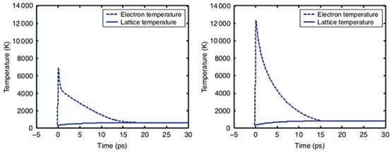
Improved models helped researchers determine the best way to shape femtosecond pulses to improve micromachining. Here are shown calculated electron and phonon temperatures of 200 nm gold film irradiated by a 140 fs, 1053 nm laser pulse at 0.2 J/cm2 via the classical model (left) and the improved model (right). (Image from Lan Jiang et al., Light: Science & Applications 2018; doi:10.1038/lsa.2017.134)
In an open paper published in Light: Science & Applications, scientists from Beijing Institute of Technology (Beijing, China), the University of Minnesota (Minneapolis, MN) and the University of Nebraska-Lincoln have summarized their research showing how shaping femtosecond laser pulses can improve the quality of the ultrafast microfabrication process. Specifically, the researchers show that the technique improves "fabrication precision, quality, throughput, and repeatability and effectively control micro/nanoscale structures."
This is not just theory; the group also provides an extensive list of experimental examples. The technique was also used to fabricate microstructures in a Chinese project (one of the 16 Chinese National S&T Major Projects). These results are the culmination of a ten-year research effort.
Electron dynamics control
Because the interaction of a femtosecond laser with a material is so short timewise, it is dominated by the photon-electron interactions themselves, rather than any resulting lattice motion, which happens on a picosecond time scale. Thus, shaping the pulses to alter these electron dynamics can alter the fabrication process. The hard part is determining what shape for what process.
To simulate electron dynamics control (EDC), the researchers used four different theoretical models: calculations for electron dynamics, a molecular dynamics simulation for phase change, a plasma model for ionization processes, and a two-temperature model for energy transport.
Based on the results, the researchers experimented with temporally and spatially shaping femtosecond pulses, creating sub-pulses that have a pulse delay shorter than the characteristic time scale of electron-lattice coupling. Based on an amplified Ti:sapphire laser from Spectra-Physics (Santa Clara, CA), the pulses in the experimental setup were shaped using a commercial 4f-configuration-based pulse shaper by Biophotonic Solutions (East Lansing, MI). The sample was mounted on a stage with a 1 μm accuracy made by PI (Karlsruhe, Germany).
Using the processes they developed, the researchers have achieved some stunning results through their project, including:
--increasing the processing efficiency of microchannel fabrication by 56 times and the maximum aspect ratio of the microchannels by three times
--boosting a laser-assisted chemical etching rate by 37 times
--adjusting the periods, orientations, and structures of surface ripples by adjusting electron generation on fabricated material surfaces
--creating Surface-enhanced Raman spectroscopy (SERS) surfaces with enhancement factors up to 1.1 × 10⁹
--fabricating deep subwavelength (~1/14 of laser wavelength) and high conductivity (~1/4 of bulk gold) nanowires in open air
The group has developed techniques to measure EDC fundamentals that includes pump-probe shadow-graph imaging technique, time-resolved plasma photography, laser-induced breakdown spectroscopy (LIBS), and a commercial fast-imaging CCD.
EDC was also used to fabricate some important prototype structures such as microholes with a diameter of 1.6 μm and an aspect ratio of 330:1.
Note: all the results above are individually referenced in the paper below. Once again, this is an open paper, so anyone can obtain it free of charge.
(From:https://www.laserfocusworld.com/articles/2018/04/shaped-femtosecond-laser-pulses-alter-electron-dynamics-to-improve-ultrafast-laser-micromachining-quality.html)