Harvard and Argonne National Lab Cooperate to Create MEMS-scanning Metalenses
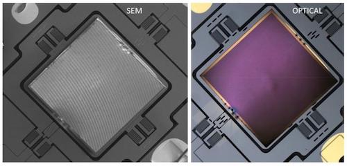
Metasurface-based flat lens is integrated onto a MEMS scanner: Scanning electron micrograph (left) and optical microscope image (right) of a lens-on-MEMS device. Integration of MEMS devices with metalenses will combine high-speed dynamic control with precise spatial manipulation of wavefronts. (Images: Center for Nanoscale Materials, Argonne National Lab)
Two technologies familiar to our audience at Laser Focus World -- metasurface lenses and MEMS -- are being united by researchers at Harvard University's John A. Paulson School of Engineering and Applied Sciences (SEAS; Cambridge, MA) and Argonne National Laboratory (Lemont, IL). Metasurface lenses are made of arrays of slowly varying, almost periodic subwavelength structures that can be lithographically fabricated on a flat surface; such a metalens, which is very lightweight, can focus monochromatic or multiwavelength light and serve other optical purposes as well. Microelectromechanical systmes (MEMS) are well-known as the technology behind digital light processing (DLP) mirror arrays, as well as many other micoromechanical components in photonics systems.
Combining metasurface lenses with MEMS can add motion capabilities like fast scanning and beam steering to metalenses for new applications.
Federico Capasso, an applied physicist at Harvard who pioneered metasurface lens technology, and Daniel Lopez, group leader of nanofabrication and devices at Argonne National Laboratory and an early developer of MEMS, have developed a device that integrates mid-infrared-spectrum metalenses onto MEMS.
"Dense integration of thousands of individually controlled lens-on-MEMS devices onto a single silicon chip would allow an unprecedented degree of control and manipulation of the optical field," says Lopez.
The researchers formed the metasurface lens using standard photolithography techniques on a silicon-on-insulator wafer with a 2-μm-thick top device layer, a 200 nm buried-oxide layer, and a 600-μm-thick handle layer. Then they placed the flat lens onto a MEMS scanner for high-speed optical-path-length modulation. They aligned the lens with the MEMS' central platform and fixed them together by depositing small platinum patches.
"Our MEMS-integrated metasurface lens prototype can be electrically controlled to vary the angular rotation of a flat lens and can scan the focal spot by several degrees," Lopez says. "Furthermore, this proof-of-concept integration of metasurface-based flat lenses with MEMS scanners can be extended to the visible and other parts of the electromagnetic spectrum, implying the potential for application across wider fields, such as MEMS-based microscope systems, holographic and projection imaging, lidar (light detection and ranging) scanners and laser printing."
When electrostatically actuated, the MEMS platform controls the angle of the lens along two orthogonal axes, allowing the scanning of the flat lens focal spot by about 9° in each direction. The researchers estimate that the focusing efficiency is about 85%.
"Such metalenses can be mass produced with the same computer-chip fabrication technology and in the future, will replace conventional lenses in a wide range of applications," Capasso says. These include miniaturized MEMS-based microscope systems, lidar scanners, and projection systems.
(From:https://www.eurekalert.org/pub_releases/2018-02/aiop-mcg022018.php)