Photonics West Preview: Dynamic, evolving, growing -- SPIE Photonics West 2018
Photonics continues to grow at a rapid pace, and the premier conference for highlighting the best the industry has to offer continues to grow as well.
GAIL OVERTON, JOHN WALLACE, and BARBARA GEFVERT
Not only have the number of symposia paper presentations increased from 4 to 7% this year with a record 5200 presentations scheduled, but exhibition floor space at SPIE Photonics West 2018 has also expanded. “The exhibition continues to grow with more square footage sold than any year in history,” says Peter Hallett, director, marketing and industry relations at SPIE (Bellingham, WA). “SPIE actually added booths in the Moscone South lower lobby to help satisfy additional demand; we sold out earlier and have a wait list of companies who took too long to book space.”
With attendance rumored to surpass the typical 20,000 of the past few years, SPIE Photonics West continues to keep pace with what makes photonics such a dynamic industry—namely, the ever-evolving scientific breakthroughs and the broad range of consumer and industrial applications that they enable.
Last year’s focus on Industry 4.0 and Internet of Things (IoT) technology has laid the groundwork for a host of photonics-enabled consumer applications that have mushroomed in importance this year, including autonomous vehicles, augmented reality/virtual reality/mixed reality (AR/VR/MR) platforms, smartphone sensing, and quantum communications—to name a few.
To be held from January 27 to February 1, 2018 at San Francisco’s Moscone Convention Center, SPIE Photonics West 2018 will once again feature the BiOS, OPTO, and LASE symposia, as well as virtual conferences on the Brain, Translational Research, and 3D Printing. The weekend BiOS exhibition features technical presentations and more than 220 exhibitors, while the Photonics West exhibition has grown to more than 1300 booths.
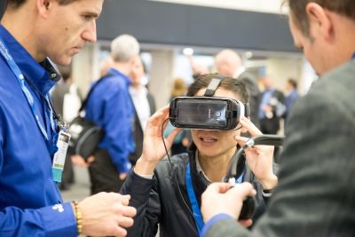
New to the conference on Monday, January 29, is the day-long Industry Event entitled “VR, AR, MR One-Day Industry Conference and Headset Demonstrations” that does exactly what it says—showcase the best altered-reality gadgets through 16 invited talks, a panel, and of course, product demonstrations (please RSVP at innovation@spie.org). The conference features not only those photonics companies with a stake in supplying products to the AR/VR/MR industry, but also the trailblazers like Google, Amazon, Microsoft, and Intel that are driving commercial applications for this technology (see Fig. 1). As Hallett explains, “Once you see what’s possible and understand what’s coming, you will have a changed view of the future.”
|
FIGURE 1. Augmented reality/virtual reality/mixed reality (AR/VR/MR) will be a focus of SPIE Photonics West 2018. (Courtesy of SPIE) |
Industry Events also include “How Global Investment Is Bringing Quantum Technologies to the Marketplace,” from 8:30 to 9:45 a.m. on Tuesday, January 30, with a comprehensive panel that discusses international funding for and commercial development of quantum communications and computing, and what types of photonic technologies will be required to move quantum development forward.
SPIE organizers want to remind potential attendees that new workshops and training courses at the conference help engineers understand both commercial solutions and the theoretical foundations that go into successful implementation of lasers, cameras, and sensors in factories, labs, and in the field. “Many technical professionals have budget for a training course every year, which can be a good way to gain approval to travel to Photonics West and increase skills early in the year,” Hallett says.
And don’t forget to socialize with your peers and mentors! Collaboration is what makes science work (and what makes it fun) and surely, you can find time for a game of pinball or Pac-Man while sipping an arcade-inspired cocktail at the conference welcome reception on Monday, January 29 from 7 to 8:30 p.m.
BiOS Symposium + Brain + Translational Research
The Biomedical Optics Symposium (BiOS) kicks off Photonics West 2018 on Saturday, January 28 with conferences organized into six tracks (Photonic Therapeutics and Diagnostics; Neurophotonics, Neurosurgery, and Optogenetics; Clinical Technologies and Systems; Tissue Optics, Laser-Tissue Interaction, and Tissue Engineering; Biomedical Spectroscopy, Microscopy, and Imaging; and Nano/Biophotonics) and two days of exhibits (10 a.m. to 5 p.m. both Saturday and Sunday).
The reliably dazzling Hot Topics plenary (Saturday, 7-9:05 p.m.) begins with the presentation of a $75,000 prize—the first-ever award of the Franz Hillenkamp Postdoctoral Fellowship in Problem-Driven Biophotonics and Biomedical Optics (see www.spie.org/hillenkamp). The new fellowship, which aims to facilitate interdisciplinary research and translation of new technologies to clinical practice, was announced in August 2017 by SPIE in partnership with four biomedical optics labs (Wellman Center for Photomedicine, the Manstein Lab in the Cutaneous Biology Research Center at Massachusetts General Hospital, Medical Laser Center Lübeck, and the Beckman Laser Institute at University of California, Irvine).
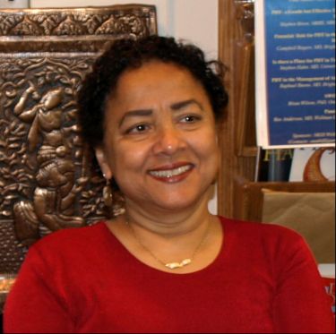
Second on the Hot Topics agenda is presentation of the 2018 Britton Chance Biomedical Optics Award, which recognizes outstanding lifetime contributions through the development of innovative, high impact bio-optics technologies (see Fig. 2). This time, the award honors Tayyaba Hasan of the Wellman Center for Photomedicine for achievements in photodynamic therapy (PDT). Dr. Hasan will start the technical presentations by highlighting PDT’s next 10 years (in 10 minutes!), after which the University of Toronto’s Brian Wilson will provide another take on PDT with his talk, “Taking the Photonics out of Photodynamic Therapy.”
|
FIGURE 2. During the BiOS Hot Topics plenary at Photonics West 2018, Dr. Tayyaba Hasan will receive the Britton Chance Biomedical Optics Award in recognition of her contributions to photodynamic therapy research. (Courtesy of SPIE) |
Then, Katarina and Sune Svanberg (of Lund University in Sweden and South China Normal University) will present on biophotonics applications of gas in scattering media absorption spectroscopy. Of the six remaining technical presentations, one is focused on noninvasive blood flow measurement (with inexpensive technology that is portable and scalable—by Turgut Durduran of ICFO, or Institut de Ciènc, in Spain). And another covers 3D multiphoton optogenetic control of neural ensemble activity (by Hillel Adesnik of the University of California/Berkeley).
The rest of the presentations report advances in imaging:
l Large-scale single-cell analysis with “extreme imaging,” presented by Keisuke Goda of the University of California/Los Angeles and the University of Tokyo (Japan);
l Oral applications of optical coherence tomography (OCT) by Julia Walther of the Technical University of Dresden (Germany);
l Label-free, morpho-functional metabolic imaging, by Irene Georgakoudi of Tufts University; and
l Brain-wide network visualization, by Qingming Luo of Huazhong University of Science and Technology (China).
A new plenary (Sunday, 3:30-5:30 p.m.) will highlight neurophotonics advances, and provide a forum for communication and networking on this topic. Organized by SPIE Brain Symposium co-chairs David Boas (Boston University) and Rafael Yuste (Columbia University), the plenary will begin with Ed Boyden of the Massachusetts Institute of Technology presenting strategies for observing and controlling neural circuits. Sergio Fantini of Tufts University will follow, with a discussion of cerebral autoregulation assessment. And then, a trio of speakers will cover clinical photobiomodulation in the brain: Michael Hamblin of the Wellman Center for Photomedicine, Elizabeth Hillman of Columbia University, and Song Hu of the University of Virginia. Finally, Na Ji of the University of California, Berkeley will present on fast, in vivo volumetric imaging of the brain before Edmund Talley of the National Institutes of Health describes funding priorities of the BRAIN Initiative.
At the third BiOS plenary (Sunday, 7-8 p.m.), Stefan Hell of Max Planck Institute (Germany) will discuss new developments on the technique that won him (and W. E. Moerner and Eric Betzig) the Nobel Prize in 2014: super-resolution fluorescence imaging, a.k.a. optical nanoscopy. Hell will focus on concepts that provide new capabilities, including molecule-scale resolution.
The now-standard Translational Research Lunchtime Forum (Sunday, 12:30-2 p.m.), a discussion of outcomes-based studies, will feature participants selected from the Translational Research virtual symposium that is integrated into the BiOS conference. Led by symposium chairs Bruce Tromberg of the Beckman Laser Institute and Medical Center at the University of California, Irvine and Gabriela Apiou of the Wellman Center for Photomedicine, Massachusetts General Hospital Research Institute, and Harvard Medical School, the speakers will demonstrate innovative optics and photonics applications with potential to improve patient outcomes.
Overlapping that by 30 minutes (Sunday, 1:30-2:30 p.m.) is a National Institutes of Health special session on funding opportunities. The program will focus on support available through the National Cancer Institute (NCI) and the National Institute of Biomedical Imaging and Bioengineering (NIBIB). Robert Nordstrom, Branch Chief for Image Guided Interventions with the Cancer Imaging Program at NCI, and Behrouz Shabestari, Program Director Optical Imaging and Spectroscopy, and Photoacoustic Imaging at NIBIB, will describe scientific programs and funding opportunities of particular importance to optical imaging and spectroscopy. In addition, Shabestari will provide an introduction to preparing and writing an NIH grant proposal for biomedical imaging and bioengineering, and discuss the NIBIB Trailblazer Award for New and Early Stage Investigators and the new R21 Exploratory/Developmental Research Grant.
BiOS poster sessions will begin Sunday (5:30-7:30 pm) and run on Monday and Tuesday evenings as well. But Monday afternoon (4:30-5:30 pm), the Journal of Biomedical Optics and Neurophotonics will host “3-Minute Poster Presentations” featuring rapid-fire overviews by students selected for one of the BiOS poster sessions. Presentations will be judged on content and presentation effectiveness by editorial board representatives of the journal, and the top three scorers will receive cash prizes.
Also on Monday (3:30-5:30 p.m.), a session titled FDA Policies and Procedures: What Academic Investigators and Small Business Should Know will offer perspectives and advice on incorporating regulatory requirements into product development, regulatory strategy success, and information on third-party review and regulatory approval for medical devices. Warren Grundfest (University of California, Los Angeles) and Ramesh Raghavachari (U.S. Food and Drug Administration) will host.
Finally, the International Biomedical Optics Society (IBOS) invites all attendees to join the Tuesday (7:30-9 p.m.) gathering that will feature a presentation describing new therapeutic strategies based on fluorescence lymphatic imaging. The nonprofit interdisciplinary group facilitates communication among medical practitioners and the scientists and engineers enabling advancements based on optics and photonics. The featured speaker is Eva M. Sevick of the Brown Foundation Institute of Molecular Medicine at Texas Medical Center, a pioneer in noninvasive fluorescence imaging of lymphatic vasculature in humans. Her tutorial will describe discovery of the “immune synapse” enabled by this technology.
LASE Symposium + 3D Printing
“The LASE program has more than 860 presentations, spanning the entire range of laser research and applications,” Hallett says. “New methods for lasers in manufacturing are especially noteworthy given great demand for everything from better batteries and aircraft engines to engineered nanostructures.”
Among the LASE highlights are the plenary presentations on Wednesday, January 31, from 10:20 a.m. to 12:35 p.m. Ursula Keller, professor at ETH Zurich (Switzerland), presents “Gigahertz Laser Frequency Combs and Dual-Comb Spectroscopy” that reviews progress on gigahertz frequency combs based on modelocked semiconductor and solid-state lasers stabilized by external silicon nitride waveguides or photonic crystal fibers (PCFs) with an f- to -2f interferometer. Her group has successfully demonstrated dual-comb spectroscopy without any active stabilization and with a single laser cavity.
The second LASE plenary presentation from RIKEN (Japan) scientist Hidetoshi Katori describes the magic-frequency protocol that has made it possible to design a new type of atomic clock with a fractional uncertainty of 10-18 based on engineered perturbations. Possible impacts and future applications of optical clocks are discussed, such as testing the fundamental laws of physics and possible redefinition of the second.
And the final LASE plenary on “Advanced Industrial Laser Systems and Applications” from Trumpf Photonics (Cranbury, NJ) CEO and president Berthold Schmidt takes a look at industrial continuous-wave (CW) laser systems, ultrashort-pulse (USP) solid-state lasers, carbon-dioxide (CO2) lasers, and disk lasers with up to 400 W average power at 343 nm—enabling such applications as extreme ultraviolet (EUV) light generation, laser lift-off, and surface annealing.
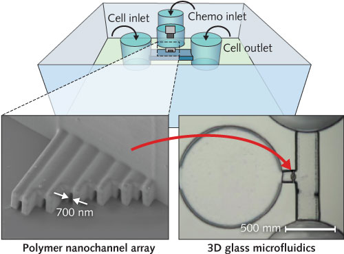
Among the numerous papers of interest are “Ship-in-a-bottle femtosecond laser integration of 3D polymer nano-channels inside a closed glass microfluidic structure for study of cancer cell migration” (paper 10521-23) from RIKEN unit leader and LASE symposium chair Koji Sugioka. This technology combines subtractive femtosecond-laser-assisted chemical etching (FLAE) of glass and additive two-photon polymerization (TPP), adding new functionality to 3D glass microfluidic biochips and enabling exploration of the mechanism of invasion and metastasis for early-stage prostate cancer (see Fig. 3).
|
FIGURE 3. “Ship-in-a-bottle” laser technology creates polymeric channels in biochips with a width of just 700 nm—the narrowest demonstrated to date for cancer cell migration studies. (Courtesy of RIKEN) |
Invited LASE papers of note include “Ablation-cooled material removal with ultrafast bursts of pulses” (paper 10522-26) from Bilkent University (Turkey), “Digital photonic production along the lines of industry 4.0” (paper 10519-6) from the Fraunhofer-Institut für Lasertechnik (Germany), and “R2R fabrication of freeform micro-optics” (paper 10520-20) from Joanneum Research Forschungsgesellschaft (Austria).
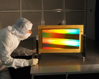
The invited talk (paper 10513-1) from Lawrence Livermore National Laboratory (LLNL; Livermore, CA) laser physicist David Alessi entitled “Pulse compression gratings for high average power petawatt-class lasers” reports on advances in diffraction gratings relevant to the HAPLS laser system that is presently being commissioned at the ELI Beamlines facility in the Czech Republic. Although pulse compressors for ultrafast lasers are typically limited to average powers below 10 W, new actively cooled gold-gratings support 600 W of average power from 10 Hz petawatt-class laser systems and multilayer dielectric gratings with broad bandwidth, low dispersion, and low absorption enable pulse compression of petawatt-peak-power laser systems operating at kilohertz repetition rates (see Fig. 4).
|
FIGURE 4. A gold-coated pulse compressor diffraction grating has been designed for high-average-power petawatt laser systems. (Courtesy of LLNL) |
Invited papers in the Tuesday afternoon “Fundamental Aspects of Laser-Materials Interaction” session from professor Baerbel Rethfeld of Technische Univ. Kaiserslautern (paper 10519-24) discuss how ultrashort laser pulses generate free electrons in dielectrics and therefore enable the absorption of laser energy, while Ben R. Torralva of the University of Michigan (paper 10519-26) explains how ultrafast lasers significantly modify the band structure of semiconductors through nonadiabatic quantum molecular dynamics simulations.
Another paper (paper 10513-32) by Fibertek (Herndon, VA) senior laser scientist Nicholas Sawruk, the “ICESat-2 Laser Nd:YVO4 amplifier,” is interesting in the sense that Fibertek is reporting on some pretty fundamental materials properties of the neodymium yttrium vanadate material system that weren’t previously known, and timely in the sense that this laser mission (which is due to launch next year) is a key enabler for monitoring global warming.
A significant number of LASE papers are understandably part of the 3D Printing virtual symposium. And on Wednesday, January 31, make time to attend the “3D Printing and Industry 4.0 Panel Session” from 8:30 to 10 a.m. that includes panelists from Trumpf, Siemens, and GE Additive. The panel explores the dramatic changes in the 3D printing/additive manufacturing landscape since the first 3D printer was created in 1984, and describes how the digitization of manufacturing—Industry 4.0—is requiring engineers to change their mindset from subtractive to additive.
Presentations in the 3D printing category attack the topic from many angles, and in fact sometimes cover the subject of 3D scanning as well as 3D printing. For example, a talk by Rudolf Verdaasdonk from the Vrije University Medical Center in the Netherlands (paper 10467-23) covers the use of 3D optical scanners for skin-prick allergy testing, quantifying the resulting skin bumps using analysis software validated with phantom bumps. Nikita Kedia of the U.S. Food and Drug Administration describes (paper 10474-12) the creation of a 3D-printed phantom of retinal photoreceptor cells for evaluating adaptive-optics (AO) retinal imaging techniques.
On the topic of 3D printing of optics, Jens Gottmann of LightFab gives an overview (paper 10522-30) of the process of selective laser-induced etching (SLE), which is a scalable subtractive 3D printing process for the creation of transparent glasses and crystals (see Fig. 5). Using SLE, precise 3D structures of fused silica have been fabricated, including microfluidic, optical, and mechanical devices. In another talk, Andreas Heinrich of Hochschule Aalen compares two different types of 3D printed optics: metal optics and polymer optics. Post-processing is discussed, including cleaning and polishing using lasers for metallic optics and dip-coating for polymer optics—in addition, examples of 3D-printed optics are given and a robot-based additive manufacturing platform is described.
|
FIGURE 5. This structure was fabricated in fused silica using selective laser-induced etching (SLE). (Courtesy of LightFab) |
In “Light controlling sound: Selective laser sintering as a tool for building aqueous acoustic metamaterials” (paper 10523-8), researchers from the U.S. Naval Research Lab discuss improvements in the quality and resolution of selective laser sintering (SLS) for metal additive manufacturing that are opening new ways to control acoustic waves in water. The speaker will outline how SLS has enabled building underwater acoustic metafluids, based on the idea that one can design an anisotropic, spatially varying stiffness tensor, while maintaining broadband single-mode propagation in a material that is acoustically impedance-matched to a background water environment.
OPTO Symposium
The three OPTO plenary presentations on Monday are concerned with two leading-edge photonics topics: silicon photonics and beating the diffraction limit. First, Andrew Rickman of Rockley Photonics (London, England) gives a talk called “Silicon Photonics: Bigger is Better” in which he discusses the idea that, unlike the shrinking feature sizes in microelectronics fabrication, maybe integrated photonics platforms can benefit from larger geometries to boost optical efficiency and ease of coupling. Next, Pallab Bhattacharya of the University of Michigan (Ann Arbor, MI) discusses the development of III-nitride (gallium-nitride-based) nanowire arrays for visible and near-infrared (near-IR) light emission on silicon for silicon photonics and other uses. Finally, Min Gu of RMIT University (Melbourne, Australia) discusses how, in his own words, “removing the diffraction limit barrier can provide a new horizon for the development of ultrahigh-capacity optical storage devices, nanoengineered topological photonics, [and] wide-angle optical displays.”
This year, the conference program tracks for OPTO include Optoelectronic Materials and Devices, Photonic Integration, Nanotechnologies in Photonics, MOEMS-MEMS in Photonics, Advanced Quantum and Optoelectronic Applications, Semiconductor Lasers and LEDS, Displays and Holography, and Optical Communications: Devices to Systems, with each track divided into a number of subtopics.
For example, Optical Components and Materials XV (Conference 10528; under Optoelectronic Materials and Devices) includes a session (paper 10528-9) by researchers at the U.S. Naval Research Lab and Sotera Defense Solutions on the development of all-crystalline double-clad fibers for high-power laser applications. These fibers can offer higher thermal conductivity and lower stimulated Brillouin scattering (SBS) thresholds and higher concentrations of dopants than glass fibers, and can potentially produce multikilowatt beam powers.
In Session 6 (Glass Fabrication and Components), Gernot Weber and Ralf Jedamzik of SCHOTT discuss the increasing use of the shortwave-IR (SWIR) region out to 4 µm (paper 10528-24), and some new IR optical glasses that transmit in the SWIR for applications such as inspection of circuit boards, bottles, food, and more.
In High Contrast Metastructures VII (under Nanotechnologies in Photonics), presenters delve into the leading-edge topic of optical metamaterials. A group at the University of Texas at Austin discusses the concept of metagratings (paper 10542-5), which they say can “tailor the flow of light with unitary efficiency and considerably lower complexity of design in comparison to conventional gradient designs.” Scientists from Caltech describe the flat optical devices they’ve been creating based on subwavelength high-index dielectric metasurfaces for free-space optics. They have developed optical systems made of several metasurfaces, which enable optical control that is hard to achieve with refractive components.
The Optical and Electronic Cooling of Solids III track includes a talk by researchers at Los Alamos National Laboratory and the University of New Mexico (paper 10550-6) on growth of crystals for “radiation-balanced lasers” (RBLs). An RBL combines solid-state optical refrigeration and lasing in one material to enable a net zero thermal load that enables scaling to high laser powers. In the same session, Arash Mafi of the University of New Mexico will describe the design and relevant parameters (gain materials, pumping schemes, and cavity design) of RBLs, with the goal of creating effective athermal lasers.
(From:http://www.laserfocusworld.com/articles/print/volume-54/issue-01/features/photonics-west-preview-dynamic-evolving-growing-spie-photonics-west-2018.html)