Novel Concept for Extreme-UV Photoresist Materials
For several years, extreme-UV (EUV) lithography—i.e., at a wavelength of 13.5nm—has been talked about as the next enabling technology for lithographic patterning. However, a number of technological stumbling blocks (i.e., issues with EUV optics, photomask infrastructures, and photoresist materials) have delayed the widespread introduction and implementation of this technique. For instance, the scanner optics that are used in patterning systems and photomasks have been changed from transmissive optics to reflective optics. This change has proven to be a rather challenging transition, but tremendous progress has now been made and EUV scanner shipments are taking place at an accelerated pace. EUV pellicle development is also progressing (a mitigation step necessary to address defect concerns), and mask infrastructures are being developed at both merchant and in-house mask shops.
To meet the requirements for new EUV-suitable photoresist materials, photoresist manufacturers originally reformulated extant 193nm resist systems—via the use of formulation adjustments, additives, and photoacid generator (PAG) loading—for EUV use. Although this is a cost-effective approach, it brings line width roughness (LWR), sensitivity, and resolution limitations. LWR is defined by the random fluctuations in the width of a patterned lithographic feature along its length. As photoresists are used to print smaller and smaller patterns, the imperfections in the sidewall become a larger part of the patterning error. Moreover, in several previous studies, these high LWR values have been attributed to the use of polymers for the photoresist matrix. Other contributing factors to the LWR values are shot noise (e.g., flux variations, which are increasingly important because the dose per photon increases substantially in the EUV regime), PAG location in the bulk film (relative to the acid-sensitive protecting group), acid diffusion (or blur) during the chemical amplification process, and the level of developer selectivity. Very few commercially available materials have an LWR below about 3nm and higher sensitivity photoresists need to be developed. For instance, most commercial photoresist systems require ∼35–40mJ/cm2 to print reasonable contact holes (with usable process windows).
About three years ago, photoresist users began to push for new photoresist platforms. ‘Molecular resists’ have thus been developed to address the concerns regarding polymer size and polydispersity, as well as concentration (related to the proximity of the acid-sensitive moieties to the PAG), and have since risen to prominence. These platforms represent a departure from conventional polymer-based photoresist suspensions and their formulations are instead based around small molecules. Indeed, there are a number of molecular systems currently being investigated for this purpose, including hafnium core nanoparticles, metal oxides, and molecular glasses. In addition, our team at Irresistible Materials have developed a new material—the multitrigger resist—which represents an evolution of our chemically amplified molecular resists. With this new approach, we can achieve high-resolution, high-sensitivity, and low-line-edge-roughness resists.
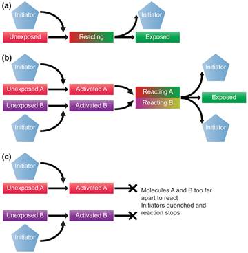
In our multitrigger materials, resist exposure proceeds via a catalytic process, in a similar manner to a chemically amplified resist: see Figure 1(a). However, instead of a single photoacid causing a single resist exposure event, in our approach, multiple photoiniatiors are necessary to activate multiple acid-sensitive molecules. These molecules then react with each other to cause a single resist event, while also causing the regeneration of the photoinitiators. In areas where there is a large number of activated photoiniators (e.g., higher dose areas at the center of a pattern feature)—see Figure 1(b)—resist components are activated in close proximity. The multistep resist exposure reaction proceeds and ends with photoinitiator regeneration, and thus further reactions, which ensures high sensitivity. In contrast, for areas with a small number of activated photoiniators (i.e., lower dose areas at the edge of a pattern feature), the activated resist components are too widely separated to react: see Figure 1(c). Active photoinitiators are thus removed, and the catalytic chain is stopped. In this way, our multitrigger concept creates an increase in the chemical gradient at the edge of patterned features and reduces undesirable acid diffusion.
Figure 1. Schematic representation of (a) the traditional chemical amplification approach used for 193 and 248nm photoresist extension materials in extreme-UV patterning. The multitrigger concept for (b) a high-dose area and (c) a low-dose area is also illustrated.
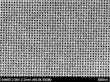
We have demonstrated our multitrigger photoresist system by printing a sample patterned with contact holes (see Figure 2). For this example, we used the Microfield Exposure Tool at Lawrence Berkeley National Laboratory, which is the world's highest resolution EUV lithography tool (0.3 numerical aperture). In particular, the patterning dose for this exposure was less than 20mJ/cm2 and the critical dimension target was dense 25nm contact hole structures.
Figure 2. Scanning electron microscope image of 25nm half-pitch contact holes. This sample was patterned on the 0.3 numerical aperture Microfield Exposure Tool at Lawrence Berkeley National Laboratory, with a patterning dose of 17.6mJ/cm2.
Our multitrigger system presents a number of benefits compared with more traditional techniques. For example, with our system we do not need to conduct a post-exposure bake (unlike most chemically amplified photoresist systems), which further enhances our process cycle time. Another advantage is that our system is carbon-based, which means that we can leverage readily available metal-reduction techniques and in-fabrication etch processes. Indeed, we are able to use extant etch processes, and can thus virtually eliminate the need for the costly and lengthy development of new etch processes. Furthermore, our partnership with Nano-C means that the required infrastructure for rapid scale-up of our multitrigger resist is already in place.
In summary, we have developed a new multitrigger photoresist for use in EUV lithography. Compared with existing photoresist systems (i.e., based on chemical amplification), our approach provides many benefits and advantages, including a low cost of ownership, high photospeed, and high resolution. Our system is also non-metallic and easily scalable for high-volume manufacturing. We have investigated all the current EUV resist testing facilities and have exhausted our cycles of learning with these test stands. We now need to examine our multitrigger resist with the use of a full-field production scanner and would welcome the opportunity to do additional testing on an ASML NXE 3XXX system. Our future focus will be on NXE patterning, LWR characterization, and image transfer analysis (pre- and post-etch pattern transfer).
(From: http://spie.org/newsroom/6883-novel-concept-for-extreme-uv-photoresist-materials?highlight=x2402&ArticleID=x126643&SSO=1)


