IMEC Exposes Wafers on NXE:3100 EUV Tool
Peter Clarke
7/11/2011 10:59 AM EDT
LONDON – Research institute IMEC (Leuven, Belgium) has said it has exposed its first wafers on the NXE:3100 extreme ultraviolet lithography preproduction tool from ASML Holding NV installed at IMEC's pilot fab.
The move is a key step towards the adoption of EUV lithography by the chip making industry as the successor to optical lithography.
The ASML NXE:3100 preproduction scanner uses a laser-assisted discharge plasma EUV light source from Xtreme Technologies, a wholly owned subsidiary of Ushio Inc. The tool shows an improvement in throughput and overlay compared to ASML's Alpha Demo Tool (ADT).
The exposure rate of the NXE:3100 is 20 times higher than that of the EUV ADT. The source power is expected to scale to 100 Watts by early 2012, increasing the scanner throughput from the current level to 60 silicon wafers per hour.
A first test of dedicated chuck overlay showed the potential to achieve the smaller than 4-nm target. At the same time, off-axis illumination options have been installed, which at factory acceptance have proven to resolve sub-20nm features using dipole illumination.
The ASML NXE:3100 is interfaced with a Lithius process track from Tokyo Electron Ltd.
"Our decision to implement the LDP source from Xtreme Technologies is an important added value for our partners since it allows them to test both our LDP and the LPP (laser produced plasma) sources currently installed at other sites," said Luc Van den hove, president and CEO of IMEC, in a statement. "We are convinced that our program will bring significant contributions to bringing EUV to mass manufacturing for the 16-nm node by 2013," he said.
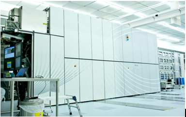
ASML NXE:3100 installed in clean room at IMEC's 300-mm pilot fab in Leuven